This document is a repository of different manufacturing tolerances. Included are tolerances listed for:
A. Injection molding
B. Sheetmetal
C. PCB Manufacture
D. Rubber Compression Molding
E. LCD fixed icon displays
F. Padprinting/silkscreening
G. Foam gaskets
I hope to add: IMD (in mold decorating), machining tolerances, magnesium-alloy and more...
http://spreadsheets.google.com/pub?key=pC0_188K00LjPE_T9BcdEHQ
Wednesday, November 28, 2007
Monday, November 26, 2007
PCB Construction

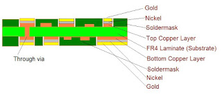
The following picture shows how a PCB is constructed. The important insights are:
(a) Soldermask provides openings that are bigger than exposed copper so that the copper will never be covered.
(b) There is only one layer of FR4 on this two layer board.
(c) Through vias are created by drilling holes through the two layers of copper and filling the through via with copper. A through via connects one layer of the board with the next. There can also be blind vias (more expensive). Also vias are designed to rest on teardrop shaped copper pads. The reason for the teardrop is for greater tolerance for the drilled hole location.
(d) Soldermask masks off the circuits on copper layers.
(e) Gold is adhered to the copper with an intermediate layer of nickel.
(f) Both the copper circuitry and soldermask is created using imagery designed by the layout person.Saturday, November 24, 2007
Subscribe to:
Comments (Atom)
